Project 3. Register
-
Given
- All the chips built Projects 1 and 2
- Data Flip-Flop(DFF gate)
-
Goal: Build the following chips:
- Bit
- Register
- RAM8
- RAM64
- RAM512
- RAM4k
- RAM16k
- PC
1-Bit Register
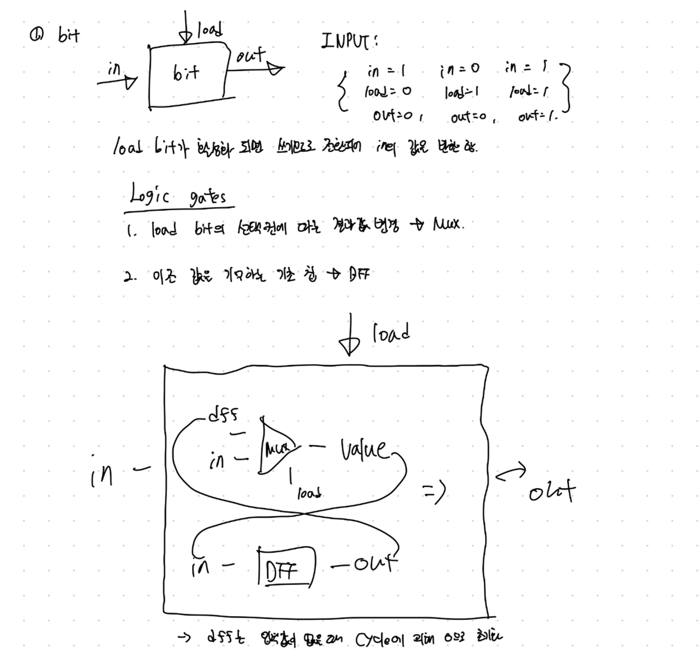
Source Code: HDL
CHIP Bit {
    IN in, load;
    OUT out;

    PARTS:
    // load bit works -> write mode.
    // first steps "a" variable has zero, because initialize.
    // write mode after, "a" variable has DFF chips output value.
    Mux(a=dff, b=in, sel=load, out=value);

    // DFF output value link MUX chip, return out
    DFF(in=value, out=out, out=dff);
}- 값을 입력 모드로 변경 하는 것은
LOAD라는 제어 비트에 의해 결정되기 때문에Multiplexor로 컨트롤 - DFF는 과거 데이터를 기억 하고 있는 형태가 된 추상적인 칩이기 때문에 Mux와 링크를 걸어 서로 연결 되어 있는 형태를 보여야 입력 모드가 아닐 때는 이전 데이터를 안정적으로 불러올 수 있음
Multi-bit Register
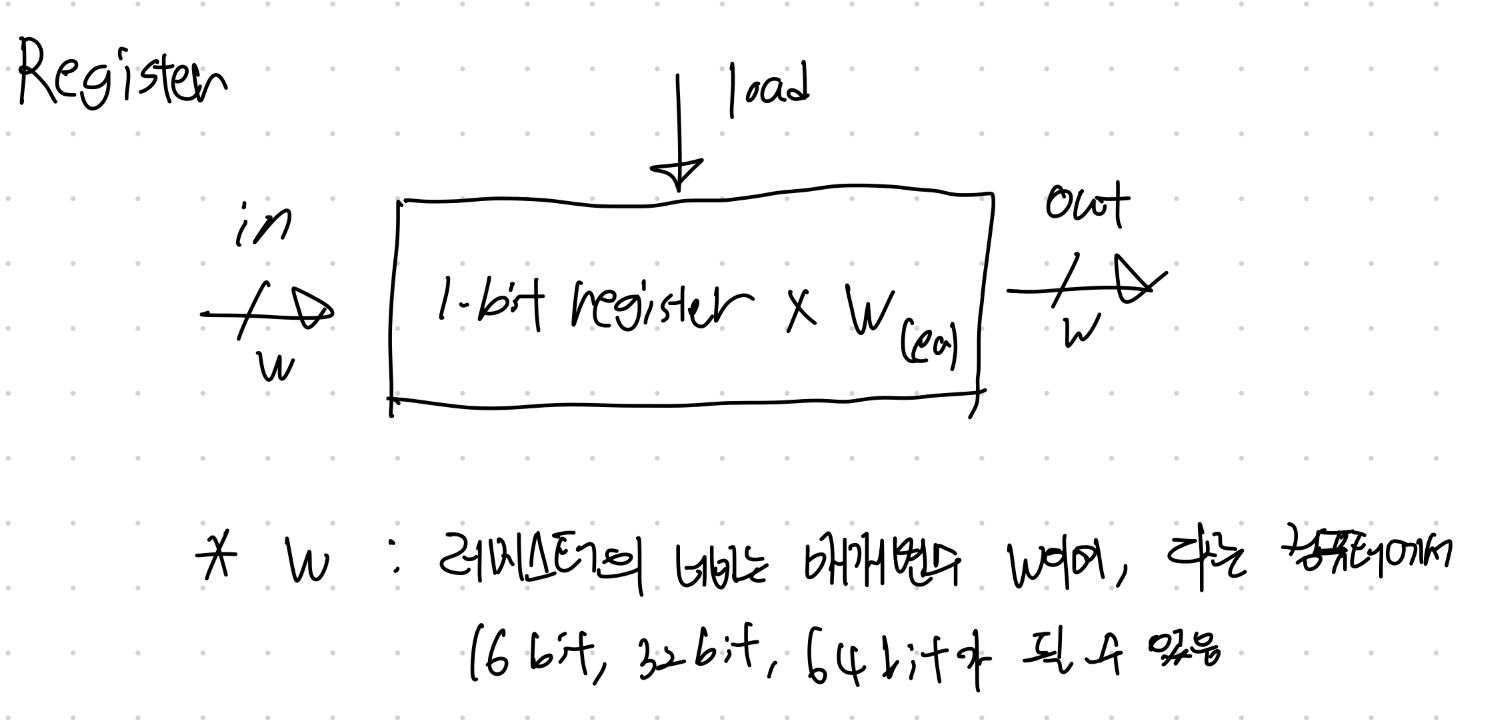
CHIP Register {
    IN in[16], load;
    OUT out[16];

    PARTS:
    Bit(in=in[0], load=load, out=out[0]);
    Bit(in=in[1], load=load, out=out[1]);
    Bit(in=in[2], load=load, out=out[2]);
    Bit(in=in[3], load=load, out=out[3]);
    Bit(in=in[4], load=load, out=out[4]);
    Bit(in=in[5], load=load, out=out[5]);
    Bit(in=in[6], load=load, out=out[6]);
    Bit(in=in[7], load=load, out=out[7]);
    Bit(in=in[8], load=load, out=out[8]);
    Bit(in=in[9], load=load, out=out[9]);
    Bit(in=in[10], load=load, out=out[10]);
    Bit(in=in[11], load=load, out=out[11]);
    Bit(in=in[12], load=load, out=out[12]);
    Bit(in=in[13], load=load, out=out[13]);
    Bit(in=in[14], load=load, out=out[14]);
    Bit(in=in[15], load=load, out=out[15]);
}
[!seealso]
- Register의 w 값 만큼 확장된 멀티 비트 레지스터 형태이다.
RAM8
-
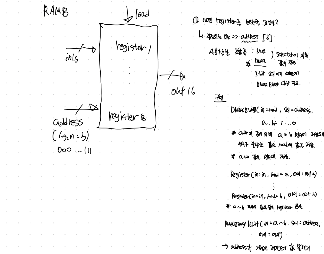
어떤 레지스터를 선택 할 것인가?
- 레지스터는 RAM 칩 내부에서 순서를 갖고 있는 저장 장치로 이 것을 결정하는 요인은
address값이 됨 address값을 이용 하여 레지스터의 위치를 나타 내기 위해서는DMux8Way를 통해3-bit address값을 가지고 8개의 레지스터 주소를 각 변수에 저장 할 수 있음- a ~ h 변수에 비트를 저장 하는 개념
- 레지스터는 RAM 칩 내부에서 순서를 갖고 있는 저장 장치로 이 것을 결정하는 요인은
-
레지스터는 값을 저장하고 있어야한다
- 8개의 레지스터는 입력 된 값이 입력모드로 되어 있다면 저장 해야함
- 그렇다면 a ~ h 의 비트 값을 불러오면 현재 레지스터가 0인지, 1인지를 판단 할 수 있음
- 8개의 레지스터는 입력 된 값이 입력모드로 되어 있다면 저장 해야함
-
모든 레지스터를 메모리 칩 내에 작동중이며 쓰는 값을 레지스터 번호에 접근 하여 언제든 저장하고 불러올 수 있어야함
CHIP RAM8 {
    IN in[16], load, address[3];
    OUT out[16];

    PARTS:
    // address has 3-bit 000... 111
    // get register seq number
    DMux8Way(in=load, sel=address, a=registerSeq1, b=registerSeq2, c=registerSeq3, d=registerSeq4,
            e=registerSeq5, f=registerSeq6, g=registerSeq7, h=registerSeq8);

    // each register do save and load
    Register(in=in, load=registerSeq1, out=outByRegister1);
    Register(in=in, load=registerSeq2, out=outByRegister2);
    Register(in=in, load=registerSeq3, out=outByRegister3);
    Register(in=in, load=registerSeq4, out=outByRegister4);
    Register(in=in, load=registerSeq5, out=outByRegister5);
    Register(in=in, load=registerSeq6, out=outByRegister6);
    Register(in=in, load=registerSeq7, out=outByRegister7);
    Register(in=in, load=registerSeq8, out=outByRegister8);

    // input value to choice register seq and load or write
    Mux8Way16(a=outByRegister1, b=outByRegister2, c=outByRegister3, d=outByRegister4,
              e=outByRegister5, f=outByRegister6, g=outByRegister7, h=outByRegister8,
              sel=address, out=out);

}
[!info]
이 후 추가적인 RAM 확장은 위 구조를 벗어나지 않기 때는다.
**구현하는 메모리 확장 종류**
- RAM64
- RAM512
- RAM4K
- RAM16K
Program Counter
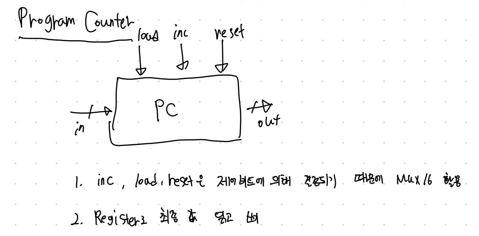
CHIP PC {
    IN in[16],load,inc,reset;
    OUT out[16];

    PARTS:
    Inc16(in=linkValue, out=incOut); // Increment

    Mux16(a=linkValue, b=incOut, sel=inc, out=modeInc);  // inc
    Mux16(a=modeInc, b=in, sel=load, out=modeLoad); // load
    Mux16(a=modeLoad, b=false, sel=reset, out=loadValue); // reset

    Register(in=loadValue, load=true, out=linkValue, out=out); // finally

}
[!info]
지금까지 해 왔던 것 처럼 제어비트에 의해 결정 되는 요소는 Multiplexor로 처리
- Register가 최종적으로 읽고 쓰는 단계를 구현하게 됨
- 그러기 위해서 레지스터의 값을 최종 결과 값과 피드백루핑 하는 값으로 나뉘어짐
- 피드백 루핑 하는 값은 절차를 타고 내려오며 하드웨어에서 레지스터가 최종적으로 내보내는 값을 기억 하고 있는 것 과 같음
Submit